Philipp Pelz
Before Philipp Pelz started as professor for computational materials microscopy at FAU Erlangen-Nürnberg, he was a postdoctoral researcher at the University of California, Berkeley, and the National Center for Electron Microscopy, US. He obtained his Ph.D. from the University of Hamburg and the Max Planck Institute for the Structure and Dynamics of Matter in Hamburg, Germany. His academic study was not only multi-disciplinary but also multi-local, with Physics, Informatics, and Applied & Engineering Physics at the Technical University of Munich, Materials Science at the University of Torino in Italy, and Chemistry at the University of Montpellier 2 in France.
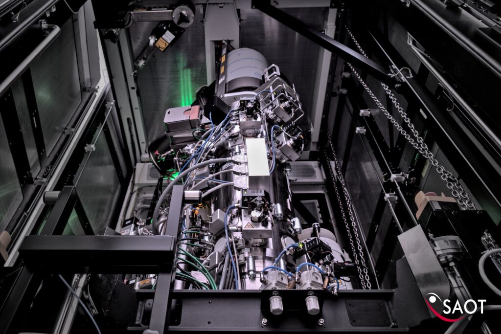
With his research, he wants to advance the capabilities of electron microscopy, a vital tool in modern materials science and engineering. So far, one can only image small volumes at atomic resolution, and especially, imaging light atoms like carbon, oxygen, and hydrogen is challenging. To overcome these, Pelz aims to develop novel methods and algorithms that will enable imaging of larger volumes with unprecedented atomic detail. This makes the study of more complex materials with excellent detail and accuracy possible.

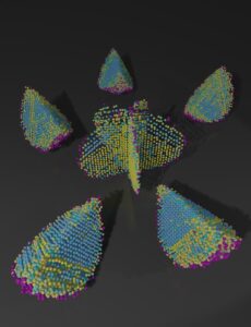
Recently awarded with a European Research Council Starting Grant in 2024, his work focuses now on advancing the imaging of atomic structures in three dimensions to larger volumes. Moreover, he will work on the visualization of the chemical composition of materials at atomic resolution and tracking changes in materials over time. This will help to understand fractures in materials leading to the development of more robust materials in the future.
My team is currently working on two main challenges: scaling our atomic-resolution imaging methods to large volumes so that they can be applied in all major sample geometries, and extracting the maximum amount of information from each interaction with the sample. This means resolving not only position and momentum but also the energy of the scattered particles we use in our microscopes. This information is used to recover the position and element of each atom in the material in 3D with high precision.

It was relatively late in my PhD. I realized that I would not be able to achieve all my goals during my doctoral studies. At the same time, I saw immense opportunities. During that time, a new generation of detectors was becoming available to electron microscopists, which allowed us to do experiments completely differently and enabled many computational imaging approaches that were impossible before. We decided to take the risk and move to the US with our kids, where such a new detector was being built.
So far, the highlight of my scientific life was realizing atomic resolution computational phase-contrast microscopy for materials science. This technique will eventually allow us to see all elements at atomic resolution and allow many insights into materials’ properties.

Moving to Erlangen allowed me to establish my own research group and continue doing the work I love.
I encourage you to look a bit beyond the horizon of your current subject. Many optics concepts can be found in different fields, with different application areas, samples, and interactions, but the underlying concepts stay the same. Examining the differences and commonalities between the disciplines is a treasure trove for research ideas.
